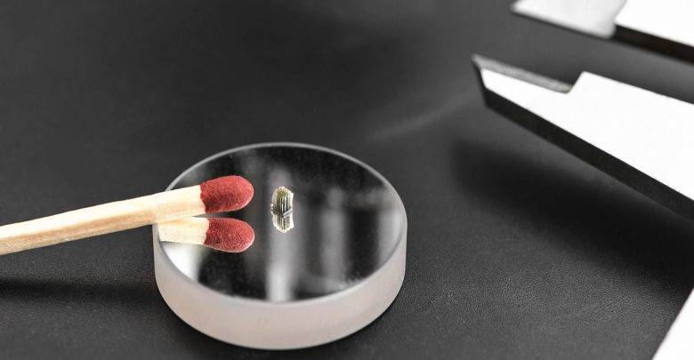
Israeli startup Nanofabrica has introduced a new micro 3D printing platform that addresses many of the challenges typically associated with nano-printing processes: cost, limited size, speed and mass production. The company says its new platform will open up numerous applications in the areas of optics, semi-conductors, microelectronics, MEMS, microfluidics and life sciences.
Founded in 2016, Nanofabrica set out to develop an additive manufacturing solution to fulfil the growing demand for parts with micron and sub-micron precision brought about by an increasing shift towards miniaturization. Though there are a number of nano 3D printing technologies in existence, the Tel Aviv company wanted to create a solution that was more accessible in terms of cost and, importantly, adaptable for volume production.
Combining DLP with adaptive optics
The result of the company’s hard work is a new end-to-end AM process capable of micron-level resolution that has an industry-friendly cost. The process uses a Digital Light Processor (DLP) engine in combination with adaptive optics to achieve repeatable micron-level resolution. The technology also integrates an array of sensors which enable a closed feedback loop. The company says it is the first to use adaptive optics in a 3D printing system.
Nanofabrica 3D printing
Array of parts made from 3 grades of ABS, 3 grades of PP and ceramic loaded parts.
Also notable about Nanofabrica’s micro AM platform is that it is capable of producing parts that are larger than competing micro or nano printing technologies—measuring over a centimeter in size. This has been achieved by leveraging adaptive optics and enhancing them using methods common in the semiconductor industry, where micron and sub-micron resolutions are achieved over similar scales. The company says that by working at the intersection of additive manufacturing and semiconductors it has been able to build macro parts with fine, micro-level details.
Variable resolutions for faster printing
The AM platform also introduces a multi-resolution strategy, which enables faster print speeds. That is, the technology prints the segments of a given part that require high resolutions slowly, to achieve accuracy, and other, less detailed portions of the component more rapidly—even up to 100 times faster. This approach reportedly allows for 5 to 100 times faster printing speeds than competing micro AM platforms.
The 3D printer can also be used for large volume production for small parts, as thousands of parts can fit into a single build. To optimize the build envelope, the technology also integrates file preparation, print orientation and support generation tools. On the materials front, Nanofabrica has developed its own range of proprietary materials, including ABS, PP and ceramics.
Nanofabrica 3D printing
A diamond shaped lattice in ABS. Part size 0.3 x 0.3 x 1mm. Print time: 45 minutes. Print layer: 3 microns.
“There are two current global trends in manufacturing. The first is the trend towards miniaturization demanding parts and components with highly precise micron and sub-micron level resolution, and the other is the move towards digital manufacturing today referred to as Industry 4.0,” commented Jon Donner, CEO of Nanofabrica. “Additive Manufacturing is a key enabling technology catering for the move towards shorter product life cycles, and allowing mass customization.
“The low set up costs associated with AM when compared to traditional manufacturing processes explains why it is now an established manufacturing technology adopted by a growing number of blue-chip companies across the world. Today, a new technology exists at the intersection of AM and micro manufacturing, opening up the possibility for manufactures to take advantage of the inherent advantages of AM while achieving micron level accuracy over a build envelope of 5 x 5 x 10cm.”
Numerous applications
In its development process, Nanofabrica identified market demands for particular applications that were either too expensive to achieve or restricted by traditional manufacturing processes. These applications fall into the categories of optics, semi-conductors, microelectronics, MEMS, microfluidics and life sciences.
Nanofabrica 3D printing
A gear made from ABS used in an inkjet industrial 2D printer. Part size 1.3 x 1.3 x 0.4mm. Print time: 35 minutes. Print layer: 2 microns.
With its ability to produce parts with micron-level resolutions as well as complex geometries and shapes, Nanofabrica’s technology is suitable for printing a range of products, including casings for microelectronics, micro springs, micro actuators, micro sensors, as well as micro valves, syringes, implantable and surgical devices for the medical sector.
Forming key partnerships
With the launch of its new micro AM technology, Nanofabrica is prioritizing the formation of partnerships with key players in its application areas. By doing so, the company aims to develop custom solutions for its partners to optimize its technology for particular applications.
The company says it is inviting prospective partners to challenge it with a specific part and to work on a proof of concept. This collaborative ethos will enable Nanofabrica and its partners to identify new opportunities for the micro 3D printing platform and ease its adoption.
Source: 3dprintingmedia.network


