About the Study
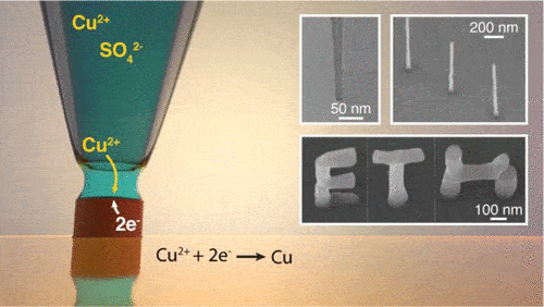
The researchers presented a unique electrochemical AM technique capable of creating 3D nanoscale features in a fully automated manner. Their printing method, which is based on rapid forming and breaking of the meniscus, offers fine control of the printing process, as well as the ability to alter the voxel size on-the-fly, and is perfectly suited for layer-by-layer nanofabrication. We approach the resolution frontier of electrochemical 3D printing with feature sizes about 25 nm by using ultrasmall nozzles with diameters as small as 1.6 nm.
Nanoscale 3D printing and requirement of new technology
Nanoscale 3D printing is gaining popularity as an alternative manufacturing technology for a wide range of applications, including electronics and nanooptics, as well as sensing, nanorobotics, and energy storage. The ever-shrinking essential dimension in cutting-edge technology necessitates the manufacturing of complex conductive devices with nanoscale resolution. Although electrochemical techniques are capable of creating impurity-free metallic conductors with excellent electrical and mechanical properties, real nanoscale resolution (100 nm) has remained elusive. In this paper, we establish a new standard in electrochemical 3D printing. We show layer-by-layer manufacture of 25 nm diameter voxels using nozzles with dimensions as tiny as 1 nm. Full control over the printing process enables on-the-fly feature size change, as well as printing tilted and overhanging structures. We estimate the limits of electrochemical 3D printing based on experimental evidence and examine the roots of this new resolution barrier.
The fabrication of complex arbitrary-shaped devices with nanoscale dimensions impacts future progress in a wide range of areas. Advanced optical technologies, sensing, micro- and nanorobotics, and more efficient energy storage all necessitate structural and functional elements with nanometer-scale feature sizes. While traditional planar fabrication procedures are frequently incapable of producing detailed 3D designs, additive manufacturing (AM), also known as 3D printing, provides immense promise for direct manufacture of complex constructions.
Among the known nanoscale 3D printing processes, stereolithography is likely the most advanced in generating complex things made up of voxels with dimensions as small as 65 nm. Optical methods, on the other hand, often process just a limited class of materials, such as photoresists, which have very limited mechanical, optical, and electrical properties. Electrically conductive structures, which are critical in many applications, have been created using a different family of technologies, such as focused electron or ion beam techniques, which have the highest AM resolution down to 8 nm. Their main disadvantage is the substantial carbon contamination caused by the organic components in the precursor gas, which frequently renders the as-printed features unsuitable for applications, particularly in sectors such as nanoelectronics or nanooptics, necessitating postprocessing.
In this regard, electrochemical AM is advantageous since it allows for the direct creation of dense conductive materials in a single step. Electrochemistry provides inherent simplicity, a high degree of control over the morphology of the resultant features, and easier impurity or composition content management. Deposition of a precursor species in a liquid bath must be limited to a small area for microscale electrochemical 3D printing. Although this enabled the creation of amazingly complex features, such as a 1:70 000 duplicate of Michelangelo’s David, greater confinement below the submicroscale in a liquid environment appears problematic. To address this issue, a liquid meniscus produced in air between a capillary tip and a substrate can be used to limit the electroplating process. Print nozzles with smaller apertures can be used to obtain lower feature dimensions. This seemingly simple concept, however, is difficult to put into reality since it necessitates great precision in syncing nozzle movement with feature growth, increasing the likelihood of tip clogging or losing the meniscus. Previous attempts to print with nanoscale nozzles failed to achieve resolutions lower than 100 nm, while the best resolution to date in printing copper structures (very conductive and extensively used in nanoelectronics) is 250 nm.
Source:


