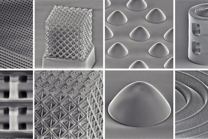
Innovation enables on-chip manufacturing for technologies in medicine, communications and other applications
A research team led by scientists at the University of California, Irvine has developed a new low-temperature method for 3D printing optical-grade glass, opening the door for microelectronic systems with high-resolution, visible-light nanophotonics capabilities.
The innovation is the subject of a paper published recently in Science.
A new generation of technologies for use in medicine, navigation, communications, remote sensing and other applications could be enabled by the combination of high-precision optics and microelectronics. But traditional methods for printing optical glass require high-temperature sintering that would cause damage to the materials that make up those very platforms.
“This work paves the way for on-chip manufacturing,” said lead author Jens Bauer, who began this project as a UCI research scientist in materials science and engineering, and who now leads the Nanoarchitected Metamaterials Laboratory at Germany’s Karlsruhe Institute of Technology. “For pretty much any chip that can sustain 650 degrees Celsius, it will be possible to print high-quality, clear glass micro- and nanostructures directly on the chip.” explained Cameron Crook, a UCI research fellow in materials science and engineering and co-author of the study.
The team’s work at UCI and KIT involved the use of a 3D-printing process called two-photon polymerization, or direct laser writing. The method enables the creation of intricate nanoscale structures but previously mostly involved formations in plastic using printer-friendly polymer resins. 3D printing with optical materials such as silica glass has required the sintering of nanoparticles at temperatures of more than 1,100 degrees Celsius, hot enough to bond materials without liquifying, but too hot for deposition on semiconductor chips.
The researchers’ solution was to use as ingredients a liquid resin built around “polyhedral oligomeric silsesquioxane,” or POSS, molecules, which contain tiny glass clusters comprised of only a handful of atoms. They combined POSS with other organic molecules to enable effortless 3D printing. The resulting crosslinked pre-glass polymeric nanostructure was heated in air to a temperature of 650 degrees Celsius, stripping off organic components to form a continuous glass nanostructure.
“The obtained glass parts of highest-ever resolution, down to 97 nanometers, were chemically perfectly pure and of optical-grade quality,” Bauer said.
He added that this technique can be adjusted to include materials beyond silica glass, unveiling entirely new powers in integrated circuits. The researchers have applied for an international patent for this innovation.
The research team included Tommaso Baldacchini at Irvine-based Edwards Lifesciences Inc. Funding was provided by the German Research Foundation, and imaging support was furnished by the UC Irvine Materials Research Institute.
Subscribe to AM Chronicle Newsletter to stay connected: https://bit.ly/3fBZ1mP
Follow us on LinkedIn: https://bit.ly/3IjhrFq
Visit for more interesting content on additive manufacturing: https://amchronicle.com


