


The semiconductor industry, known for its precision and innovation, has experienced a significant shift toward advanced manufacturing techniques. Metal additive manufacturing (AM), also known as metal 3D printing, is emerging as a critical tool in this domain. The ability to create complex geometries, rapid prototyping, and customization has driven a surge in the demand for metal additive manufacturing in semiconductor production and research.
Top Reasons Why Metal AM Demand Is Increasing in the Semiconductor Industry
The semiconductor industry operates in a highly competitive and fast-paced environment, requiring constant innovation. Metal additive manufacturing allows for complex geometries and intricate designs that traditional manufacturing methods struggle to achieve. This capability is essential for creating advanced semiconductor components and heat sinks with intricate cooling channels.
In the semiconductor industry, rapid development cycles are crucial. Metal AM enables faster prototyping, allowing engineers to quickly test and iterate on designs. This speed can significantly reduce time-to-market and costs associated with product development. Metal additive manufacturing supports customized production, which is increasingly important in semiconductor applications. Custom fixtures, tooling, and specialized components can be manufactured on-demand, allowing for more flexible and cost-effective production processes.
Traditional subtractive manufacturing methods can generate significant material waste. Metal AM is additive, using only the material required for each part, leading to less waste and reduced material costs. The ability to manufacture metal components on-site or in localized facilities reduces supply chain risks and transportation costs. This aspect is particularly relevant in a globalized industry like semiconductors, where supply chain disruptions can impact production schedules.
Applications and Use Cases
Metal additive manufacturing is finding applications across the semiconductor industry, including heat sinks and thermal management, custom tooling and fixtures, microwave and RF components and prototyping and testing.
Semiconductor devices generate significant heat, requiring effective thermal management. Metal AM enables the design and production of complex heat sinks and cooling structures tailored to specific requirements. Custom fixtures and tooling are often needed for semiconductor manufacturing. Metal additive manufacturing allows for the rapid production of these components, reducing lead times and increasing flexibility.
The ability to create intricate and precise geometries makes metal AM suitable for manufacturing microwave and RF components used in semiconductor applications. Metal additive manufacturing is also used for creating prototype components and specialized testing equipment, enabling semiconductor manufacturers to iterate quickly during product development.
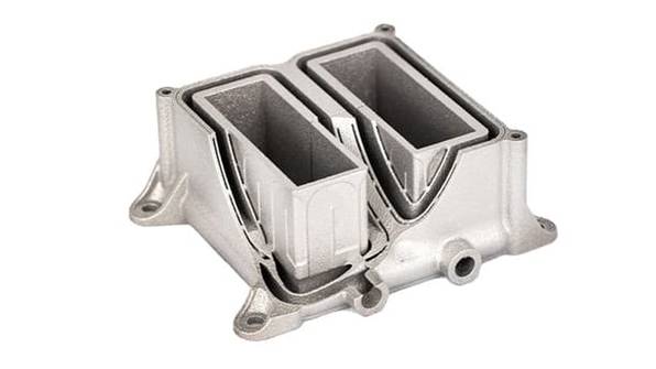
Fluid Flow Optimization
Semiconductor processes often involve complex fluid dynamics, requiring precise flow control for cooling, chemical delivery, and other applications. Metal AM allows engineers to design and produce intricate internal geometries, optimizing fluid flow and improving system performance. For example, fluid channels with complex curvatures and varying diameters can be manufactured using metal AM to enhance cooling efficiency and ensure even distribution of fluids.

Structural Optimization
Semiconductor manufacturing equipment often requires robust yet lightweight structures. Metal additive manufacturing enables topology optimization, where material is added only where needed for structural integrity. This approach reduces overall weight, improves mechanical performance, and allows for innovative designs that would be impossible with traditional methods.
Wafer Table Thermal Management
In semiconductor fabrication, maintaining stable temperatures is critical for process control. Metal AM can create customized wafer tables with integrated cooling channels, allowing for efficient thermal management. These designs can be tailored to specific process requirements, ensuring uniform temperature distribution across the wafer and enhancing overall production quality.
Linear Stage Cooling
Linear stages are essential for precise movement in semiconductor manufacturing. Metal additive manufacturing enables the creation of cooling systems integrated into linear stages, reducing thermal expansion and maintaining accuracy during high-precision operations. This integration can lead to improved stage performance and extended lifespan.
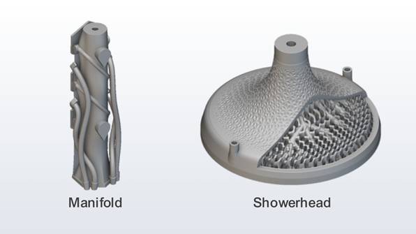
Showerhead Optimization
Showerheads play a crucial role in semiconductor manufacturing, distributing gases evenly across wafers. Metal AM allows for highly customized showerhead designs with intricate internal structures to ensure optimal gas distribution and mixing. This capability can lead to more uniform deposition and improved process results.
Gas Conveyance and Mixing
The efficient conveyance and mixing of gases are vital for many semiconductor processes. Metal additive manufacturing can create complex internal geometries within gas conveyance systems, optimizing flow paths and promoting better gas mixing. This flexibility enhances process consistency and reduces the risk of defects caused by uneven gas distribution.
Limitations
Despite its numerous advantages, metal additive manufacturing in the semiconductor industry has some limitations. The initial investment for metal additive manufacturing equipment can be high. This cost barrier may limit adoption among smaller companies or those with limited budgets. While metal AM can work with various metals, certain specialized materials used in semiconductor manufacturing may not yet be compatible with existing AM technologies. Metal additive manufacturing may require additional post-processing to achieve the desired surface finish and accuracy, adding time and cost to the production process. Some metal AM systems have limitations on the size of parts they can produce, potentially restricting their use in certain semiconductor applications.
Conclusions and Future Scope
Metal additive manufacturing is rapidly gaining ground in the semiconductor industry, offering design flexibility, rapid prototyping, customization, reduced waste, and localized production benefits. While there are limitations, such as the high cost of equipment and the need for post-processing, the technology’s advantages often outweigh these drawbacks.
The future scope of metal additive manufacturing in the semiconductor industry is promising. As technology advances and costs decrease, broader adoption is likely. Innovations in materials and processing techniques will further expand the applications of metal AM, enabling the production of more complex and precise semiconductor components. Additionally, as sustainability becomes increasingly important, the reduced material waste and energy efficiency of metal additive manufacturing will play a crucial role in the industry’s continued growth.
Overall, metal additive manufacturing is poised to become a cornerstone of semiconductor manufacturing, driving innovation and efficiency in the years to come.
Sources:
1. Revolutionizing Semiconductor Equipment Manufacturing, By Oerikon AM
2. Additive Manufacturing for Semiconductor Capital Equipment, By 3D Systems


